AMADA Micro Welding Section
Systems
Semiconductors
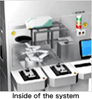
Wafer Marking System

Small footprint.
This system is for marking on wafers; silicon wafer, sapphire substrate, and compound wafer.
- Small footprint.
- Highly precise marking.
- High throughput.
Features
- ■ White marking: by SHG laser
-
It melts only surface of a silicon wafer, so marking can be done without particles.

- ■ Black marking: by fundamental laser
-
It engraves surface of a silicon wafer. Marked workpiece has a high level of visibility and can be read clearly even after cleansing and grinding.
-
![Black marking: by fundamental laser]](/media/images/products/img_wafer_02.jpg)
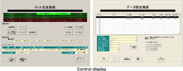
* Please contact a sales person for details.
Customer support
If you have any questions as the products, reparing, and corporate information, plaese contact us.
Customer support